
TL;DR
Longi and Yangzhou University have developed a laser manufacturing process that produces a heterojunction back-contact solar cell with 27.27% efficiency. This breakthrough addresses laser-induced damage issues and offers a pathway to ultra-high-efficiency photovoltaics.
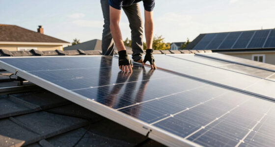
Researchers from Longi and Yangzhou University have developed a new laser-based manufacturing process for heterojunction back-contact solar cells, achieving a certified efficiency of 27.27%. This breakthrough addresses long-standing challenges related to laser-induced damage, potentially advancing commercial high-efficiency photovoltaic production.
The team employed a laser mitigation strategy targeting shock-wave damage caused by ultrafast laser pulses during rear-side patterning. They identified the silicon nitride (SiNx) layer as a primary source of damage, where non-thermal ablation driven by ultrafast energy deposition generates shock waves that can impair cell performance. By analyzing device architectures with and without the SiNx layer, they confirmed that shock waves reflect and amplify stress at the pyramid tips, causing microcracks and passivation failure.
To counteract this, the researchers experimented with different front-side textures, notably submicron, rounded-top pyramids, which significantly reduced stress concentration and improved passivation stability. The best-performing cell achieved a power conversion efficiency of 27.27%, with an open-circuit voltage of 745.0 mV, a short-circuit current of 7,439 mA, and a fill factor of 86.19%. This performance is close to Longi’s previous record of 28.13%, confirmed by the Institute for Solar Energy Research Hamelin (ISFH). The findings suggest that strategic surface engineering can enable high efficiency while mitigating laser damage during manufacturing.
Implications for Commercial High-Efficiency Solar Manufacturing
This development is significant because it demonstrates a practical pathway for producing ultra-high-efficiency heterojunction solar cells at industrial scale. By addressing laser-induced shock wave damage, the technique could improve manufacturing yields and device stability, potentially lowering costs and accelerating adoption of high-performance photovoltaics.
While the efficiency achieved is close to the current world record, the process’s scalability and integration into existing production lines remain to be validated. If successful, it could influence future solar cell manufacturing standards and enable more widespread deployment of high-efficiency modules.

Callsun N-Type 16BB 400W Bifacial Solar Panel, 2Pcs 200 Watt Solar Panel 12V, 25% High Efficiency, Dual-Module Parallel Anti-Shade Design, for RV Van Marine Home Rooftop Off-Grid Systems
【N-Type 16BB High-Efficiency Solar Cells】The Callsun 200 watt solar panel is built with advanced N-type solar cells and…
As an affiliate, we earn on qualifying purchases.
As an affiliate, we earn on qualifying purchases.
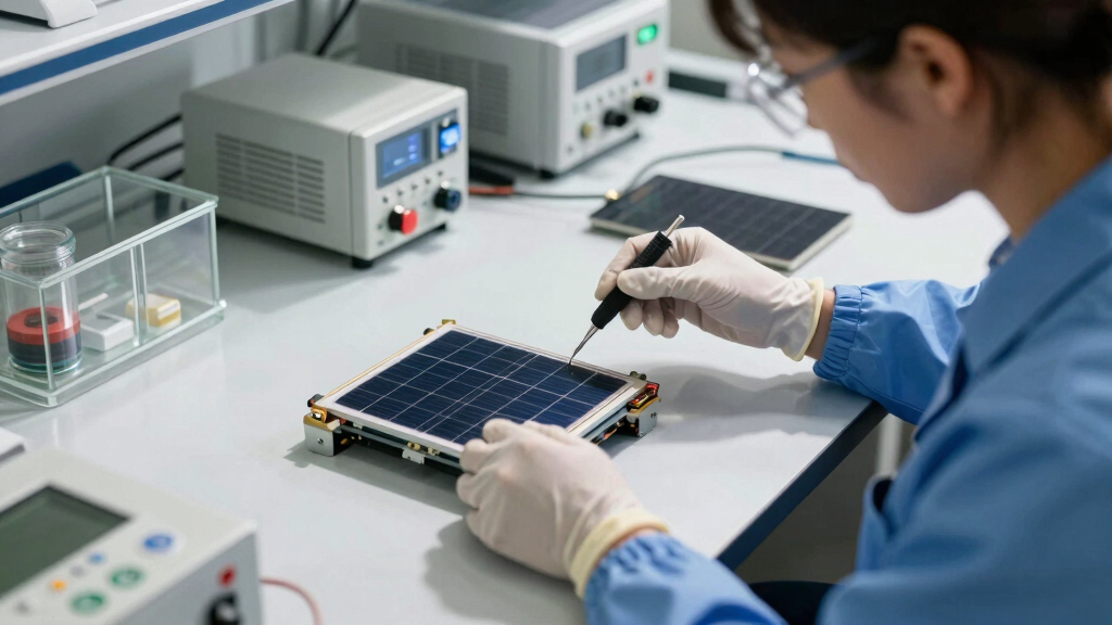
Advances in Laser Processing for Photovoltaics
Laser processing is increasingly used in photovoltaic manufacturing for patterning and contact formation due to its precision and throughput benefits. However, high-energy laser pulses can induce shock waves that damage silicon wafers, limiting the maximum achievable efficiency and device reliability. Previous efforts to mitigate laser damage have focused on process adjustments, but challenges persisted in balancing speed, quality, and device performance.
This new research builds on prior studies by identifying the SiNx layer as a key factor in shock-wave amplification and demonstrating how surface texture modifications can reduce stress concentration. Longi’s previous high-efficiency heterojunction cells reached approximately 28.13%, but manufacturing challenges related to laser damage remained a barrier to further improvements.
“Our work not only addresses a major contradiction in laser-based manufacturing but also offers a practical, industry-ready route toward ultra-high-efficiency photovoltaics.”
— an anonymous researcher
High-Efficiency Crystalline Silicon Solar Cells
As an affiliate, we earn on qualifying purchases.
As an affiliate, we earn on qualifying purchases.
Unconfirmed Aspects of Manufacturing Scalability
It remains unclear how easily this laser mitigation technique can be scaled for mass production and whether it will be compatible with existing manufacturing infrastructure. Further testing is needed to confirm long-term stability and cost-effectiveness in commercial settings.

Solar Label Pack- 6X-Warning Electric Shock Hazard-The DC Conductors of This PHOTOVOLTAIC System are UNGROUNDED and May BE Energized-4’’ X 3’’
Strong & Permanent Adhesive
As an affiliate, we earn on qualifying purchases.
As an affiliate, we earn on qualifying purchases.
Next Steps for Industry Adoption and Validation
Further research will focus on integrating the laser mitigation process into large-scale production lines, testing long-term device stability, and verifying cost benefits. Longi and partners are likely to pursue pilot manufacturing runs and seek industry collaborations to commercialize this technology.

Solar Panel Coating | Anti Dust | Self-Cleaning | Anti-Soiling | Anti-Snow | Hydrophobic | Graphene Infused | Anti-Abrasion | Protection up to 5YRS | 10H Hardness | Eco-Friendly | Ceramic Coating
✅Maximizes solar power generation by enhancing sunlight penetration and preventing power losses from dust and dirt accumulation.
As an affiliate, we earn on qualifying purchases.
As an affiliate, we earn on qualifying purchases.
Key Questions
How does the new laser process improve solar cell efficiency?
The process reduces laser-induced shock wave damage, allowing for higher-quality passivation and more stable device architecture, which contributes to higher efficiency.
Can this manufacturing method be applied to other types of solar cells?
While developed for heterojunction back-contact cells, the principles may be adaptable to other laser-processed photovoltaic devices, but further research is needed.
What are the main technical challenges remaining?
Scaling the process for industrial throughput, ensuring long-term device stability, and integrating new surface textures into existing production lines are key challenges ahead.
How close is this to commercial deployment?
The efficiency achievement is near the current record, but industrial-scale validation and cost analysis are still required before commercial adoption.
Source: PV Magazine